How To Apply Telecentric Lenses In PCB Printing
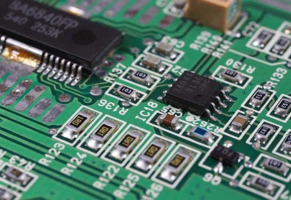
With the rapid development of the electronics industry, PCB (printed circuit board), as the carrier of electrical connection of electronic components, has higher and higher manufacturing quality requirements.The development trend of high precision, high density and high reliability makes PCB inspection particularly important.
In this context, telecentric lens, as an advanced visual inspection tool, is increasingly widely used in PCB printing, providing a new innovative solution for PCB inspection.
1、Working principle and characteristics of telecentric lens
Telecentric lenses are designed to correct the parallax of traditional industrial lenses. Their characteristic is that the image magnification does not change within a certain object distance. This characteristic makes telecentric lenses have unique advantages in PCB inspection.
Specifically, the telecentric lens adopts a telecentric optical path design, which is divided into an object side telecentric optical path and an image side telecentric optical path.
The object side telecentric optical path can eliminate the reading error caused by inaccurate focus on the object side, while the image side telecentric optical path can eliminate the measurement error introduced by inaccurate focus on the image side.
The bilateral telecentric optical path combines the dual functions of object side and image side telecentricity, making the detection more accurate and reliable.
Application of telecentric lens in PCB inspection
2、Application of telecentric lens in PCB inspection
The application of telecentric lenses in PCB inspection mainly includes the following aspects:
PCB vision alignment system
PCB visual alignment system is a key technology to realize automatic scanning and positioning of PCB. In this system, telecentric lens is a key component that can image the target on the photosensitive surface of the image sensor.
By using a web camera and a high-field-of-field telecentric lens, you can ensure that the product can produce clear images within a certain height, and its performance is stable and reliable. This solution not only improves the detection accuracy, but also greatly improves production efficiency.
High-precision defect detection
Defect detection is a key part of the PCB manufacturing process. The high resolution and low distortion characteristics of the telecentric lens enable it to accurately capture tiny defects on the circuit board, such as cracks, scratches, stains, etc., and combined with image processing software, it can realize automatic identification and classification of defects, thereby improving detection efficiency and accuracy.
Component position and size detection
On PCBs, the position and size accuracy of electronic components have a significant impact on product performance. Telecentric lenses ensure that the image magnification remains constant during the measurement process, enabling accurate measurement of component position and size.
This solution not only improves measurement accuracy, but also helps optimize production processes and improve product quality.
Welding quality control
During PCB soldering, telecentric lenses can be used to monitor the soldering process including the shape, size and connection of solder joints. Through the magnified field of view of the telecentric lens, operators can more easily detect possible problems in soldering, such as excessive or insufficient melting of solder joints, inaccurate soldering positions, etc.
Final Thoughts:
If you are interested in purchasing various types of lenses for surveillance, scanning, drones, smart home, or any other use, we have what you need. Contact us today to learn more about our lenses and other accessories.
Click here to view more telecentric lens content:
Specific Applications Of Telecentric Lenses In Scientific Research Fields
The Function And Common Application Areas Of Telecentric Lenses
